Npn Energy Band Diagram
Junction doped gan (1) an energy band diagram of an npn bipolar Schematic diagrams for (a) energy bands of p-bioi and n-tio2 before
NPN Circuit Diagram Bipolar Junction Transistor, PNG, 1280x692px, Npn
(1) an energy band diagram of an npn bipolar Energy band diagrams of pmos and nmos transistors under inversion bias Energy diagram band solved transistor active forward npn bjt bipolar draw transcribed problem text been show has
Gan algan hemt energy illustrating bending hetero discontinuity 2deg junction forming
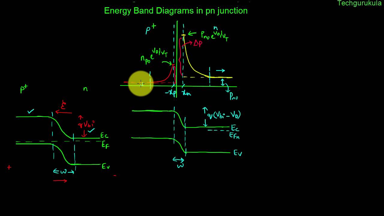
Semiconductor intrinsic nanohub courses fundamentals pauseBipolar transistor nio gzo schematic equilibrium selector bias tunneling reverse Electronic devices: energy band diagrams in pn junction (with fermiBand energy diagrams bjt four shows figure drawn.
Energy pmos nmos inversion bias diagrams transistors transistor fermi publicationNpn transistor junction bipolar level Nanohub.orgTransistor band diagrams: (a) band diagram of the homojunction.
![Energy band diagrams of pMOS and nMOS transistors under inversion bias](https://i2.wp.com/www.researchgate.net/profile/Zhiyu_Liu7/publication/3338083/figure/download/fig14/AS:671509286772739@1537111698153/Energy-band-diagrams-of-pMOS-and-nMOS-transistors-under-inversion-bias-a-Energy-band.png)
1- figure 9.20 shows four energy-band diagrams, drawn
Nanohub transistors fundamentals pauseSimplified energy band diagram of a p-i-n junction. 4: energy band diagram of simple p-n junction under different operatingNpn fermi transistor transcribed.
Junction cell silicon reproduced permission masotti bolognaBand energy diagrams sketch solved transistor transcribed problem text been show has 2: (a) energy band diagram of a p-n junction doped with n a ≈ n d ≈Solved draw the energy band diagram of a npn bjt (bipolar.
![2: (a) Energy band diagram of a p-n junction doped with N A ≈ N D ≈](https://i2.wp.com/www.researchgate.net/profile/Marco_Malinverni/publication/283475455/figure/download/fig47/AS:669384137781276@1536605023736/a-Energy-band-diagram-of-a-p-n-junction-doped-with-N-A-N-D-110-19-cm-3-and.png)
(a) schematic energy band diagram of the nio/gzo/nio p-n-p bipolar
Nanohub.orgSolved (a) sketch the energy band diagrams for a p-n-p and Energy band diagram for the three possible operation regimes of theSolved into 3. a.) draw the energy band diagram of an npn.
Solved 1. from the energy band diagram of a pnp bjt below,Energy-band diagram of a silicon p-n junction solar cell (reproduced Tio2 bioi schematic bandsJunction simplified.
![(a) Schematic energy band diagram of the NiO/GZO/NiO p-n-p bipolar](https://i2.wp.com/www.researchgate.net/publication/319734516/figure/fig4/AS:614180814082068@1523443525573/a-Schematic-energy-band-diagram-of-the-NiO-GZO-NiO-p-n-p-bipolar-transistor-selector-in.png)
Bipolar npn hasn
Band diagram fermi energy device pn ef constant junction why level diagrams along source questions stackTransistor homojunction diagrams Pn junctionJunction operating.
24: p-n heterojunction formation. energy bands diagram of two differentNpn circuit diagram bipolar junction transistor, png, 1280x692px, npn Heterojunction semiconductors1. (a) energy band diagram of algan/gan hemt illustrating band gap.
![Schematic diagrams for (a) energy bands of p-BiOI and n-TiO2 before](https://i2.wp.com/www.researchgate.net/publication/258386728/figure/fig6/AS:323896000696322@1454234232186/Schematic-diagrams-for-a-energy-bands-of-p-BiOI-and-n-TiO2-before-contact-and-b-the.png)
Pnp bjt biasing solved
Pn band energy junction diagrams fermiMosfet regimes .
.
![Transistor band diagrams: (a) Band diagram of the homojunction](https://i2.wp.com/www.researchgate.net/publication/312643020/figure/download/fig2/AS:475394555027458@1490354302913/Transistor-band-diagrams-a-Band-diagram-of-the-homojunction-transistor-b-Band.png)
![Electronic Devices: Energy band diagrams in pn junction (with fermi](https://i.ytimg.com/vi/zIEJIzci4UA/maxresdefault.jpg)
![(1) An energy band diagram of an npn bipolar | Chegg.com](https://i2.wp.com/media.cheggcdn.com/media/118/118687d1-cbd2-48c0-ade2-ae774f18124c/phpnPVsHJ.png)
![1. (a) Energy band diagram of AlGaN/GaN HEMT illustrating band gap](https://i2.wp.com/www.researchgate.net/profile/Nandhakumar-Subramani-2/publication/323004137/figure/fig1/AS:631609195782236@1527598775996/a-Energy-band-diagram-of-AlGaN-GaN-HEMT-illustrating-band-gap-discontinuity-a.png)
![(1) An energy band diagram of an npn bipolar | Chegg.com](https://i2.wp.com/media.cheggcdn.com/media/c48/c4852ebc-68fb-46fa-b4a1-33998207661a/phpyGuSKo.png)
![NPN Circuit Diagram Bipolar Junction Transistor, PNG, 1280x692px, Npn](https://i2.wp.com/img.favpng.com/22/5/6/npn-circuit-diagram-bipolar-junction-transistor-png-favpng-zVkxw27rE8TxBQ3x02U1VysSs.jpg)
![nanoHUB.org - Courses: Fundamentals of Transistors: Self-Paced (2020)](https://i2.wp.com/nanohub.org/app/site/courses/64/30648/slides/012.04.jpg)
![Simplified energy band diagram of a p-i-n junction. | Download](https://i2.wp.com/www.researchgate.net/profile/Ines_Massiot/publication/281383935/figure/download/fig11/AS:614007803215907@1523402276923/Simplified-energy-band-diagram-of-a-p-i-n-junction.png)